
Modern pharmaceutical compounding suites, semiconductor cleanroom airlocks, and regulated medical device assembly lines operate under strict FDA 21 CFR Part 11 and EU Annex 11 electronic signature mandates. Shared passwords and easily borrowed RFID badges fail regulatory audit scrutiny when operators approve critical batch recipe changes. Integrating a high-resolution biometric fingerprint scanner directly into the front bezel of a compact 10.1-inch industrial panel PC (16:10 / 1280×800 resolution) enforces non-repudiable operator authentication without external USB dongles.
⚡ Engineering Executive Summary (Key Technical Takeaways):
- Sub-Femtofarad Capacitive Sensing: 508 DPI active RF capacitive sensor resolves 0.332 fF ridge-to-valley capacitance differentials, authenticating dry, damp, or worn factory fingertips in < 250 ms.
- Live-Finger Anti-Spoofing: Sub-epidermal RF impedance verification rejects silicone or gelatin fake prints while passing FDA 21 CFR Part 11 audit trails.
- ±15 kV ESD Bezel Shunting: Grounded stainless sensor ring diverts high-voltage static discharges safely to chassis earth before transients reach the mainboard.
However, deploying capacitive fingerprint sensors on industrial shop floors introduces severe electrical and environmental challenges. Dry cleanroom air generates high electrostatic charges on operator fingers, while optical sensors fail when ambient overhead lights fluctuate or fingers carry faint skin oils. Engineering a dependable terminal across modern cleanroom hmi access-control stations requires analyzing active RF capacitive ridge-valley physics, grounded ESD bezel shunting, and sealed front glass integration.
1. Active RF Capacitive Ridge-Valley Sensing & Sub-Femtofarad Resolution
Unlike optical prism scanners that suffer from ambient light glare and surface scratches, an active RF capacitive fingerprint array measures microscopic air-gap capacitance differentials between epidermal ridges and valleys across a 508 DPI pixel matrix:
Micro-Capacitive Ridge-to-Valley Differential Equation: Parallel-Plate Micro-Pixel Capacitance: C_pixel = (ε_0 × ε_r × A_pixel) / d_gap Where: – Permittivity of Free Space: ε_0 = 8.854 × 10^-12 F/m; Air Dielectric: ε_r ≈ 1.0. – 508 DPI Sensor Pixel Area (50 μm × 50 μm): A_pixel = 2.50 × 10^-9 m². – Epidermal Ridge Distance (Through Hard Protective Coating): d_ridge = 50 μm = 5.0 × 10^-5 m. – Epidermal Valley Distance: d_valley = 200 μm = 2.0 × 10^-4 m. Ridge vs. Valley Capacitance Calculation: C_ridge = (8.854 × 10^-12 × 1.0 × 2.50 × 10^-9) / (5.0 × 10^-5) ≈ 0.443 fF (femtofarads). C_valley = (8.854 × 10^-12 × 1.0 × 2.50 × 10^-9) / (2.0 × 10^-4) ≈ 0.111 fF. Differential Signal: ΔC = C_ridge – C_valley = 0.332 fF. Signal Processing: A 24-bit Sigma-Delta ADC with a sub-0.01 fF noise floor resolves ΔC with > 30 dB SNR while sub-epidermal RF excitation verifies live human tissue impedance.
Because active RF excitation penetrates dead outer skin layers to map the live dermal boundary, the sensor achieves a False Acceptance Rate (FAR) below 0.001% even on dry or lightly abraded operator hands.
To enforce single-touch operator accountability and eliminate trailing USB fingerprint readers, pharmaceutical and manufacturing engineers deploy the 10.1″ Biometric Fingerprint Industrial Panel PC (Access Control), which integrates a flush-mounted capacitive scanner directly into the lower front bezel.
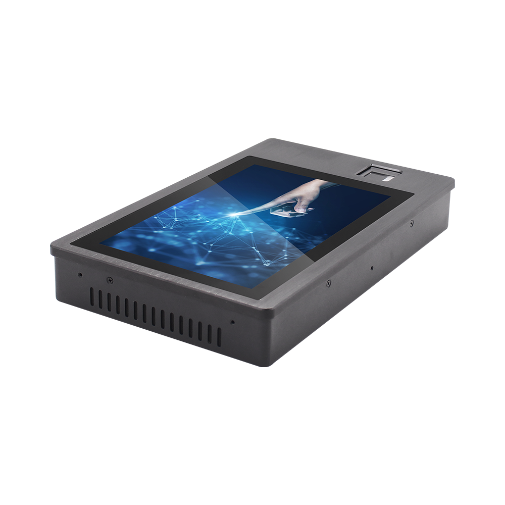
10.1″ Biometric Fingerprint Industrial Panel PC
Designed for FDA 21 CFR Part 11 cleanroom MES stations, airlock access control, and secure machine login. Features an integrated 508 DPI active RF capacitive fingerprint sensor, ±15 kV ESD grounded ring, IP65 front sealing, and 100% fanless cooling.
2. ±15 kV Electrostatic Discharge (ESD) Ring & Sealed Bezel Architecture
Protecting sensitive biometric electronics in dry cleanrooms and factories requires strict electrostatic and ingress engineering:
- Grounded Metallic ESD Bezel Ring: Surrounding the sensor die is a conductive stainless bezel ring bonded directly to chassis ground, discharging up to ±15 kV human-body static zaps before the finger touches the active silicon array.
- IP65 Front Washdown & Chemical Wipe Immunity: The sensor surface is coated with a diamond-like carbon (DLC) protective layer (> 8H hardness) and sealed flush with the front glass, withstanding daily 70% IPA sanitizer wipes.
- Compact 10.1″ Fanless Enclosure: Fits cleanly onto cleanroom airlock mullions, machinery control doors, and time-attendance kiosks without ventilation slots that trap airborne particulates.
External USB Fingerprint Dongle vs. Engineered 10.1″ Biometric Panel PC
| Security & Hardware Factor | Desktop USB Optical Scanner | INNODA 10.1″ Biometric Panel PC |
|---|---|---|
| Sensing Technology | Optical prism (Fails on dry/oily fingers & glare) | 508 DPI active RF capacitive live-tissue sensor |
| ESD Static Immunity | ±4 kV (Crashes USB bus on winter static shock) | ±15 kV air / ±8 kV contact grounded ESD ring |
| Front Washdown Sealing | Unsealed plastic shell (Traps cleanroom dirt) | IP65 flush-sealed front bezel (IPA wipeable) |
| Physical Tamper Security | Unplugged or stolen from USB port easily | Internally hardwired bus inside locked cabinet |
| Sensor Surface Durability | Soft plastic window clouds with alcohol wipes | 8H Diamond-Like Carbon (DLC) scratch-proof coat |
3. Commissioning & Biometric Enrollment Best Practices
- Dual-Finger Template Enrollment: Enroll both primary index and middle fingers per operator at 500+ DPI during onboarding to guarantee instant sub-250 ms authentication even if one finger wears a bandage.
- Chassis Earth Ground Verification: Bond the rear chassis ground lug to the facility star ground bus (≤ 0.1 Ω) so the front ESD bezel ring dissipates static charges effectively.
- Periodic Sensor Surface Decontamination: Wipe the capacitive sensor window at shift end with a lint-free swab dampened with 70% isopropyl alcohol to remove skin lipids without leaving residue.
Standardizing regulated cleanroom airlocks and MES operator terminals on 10.1-inch biometric fingerprint industrial panel PCs strengthens FDA audit compliance and eliminates external peripheral failures. Contact INNODA’s biometric HMI engineering team to request Windows/Android biometric SDK libraries, 3D STEP cutout drawings, and evaluation units.